Sometimes you won’t always have access to the correct footprint, or it may not even exist. This does not mean you have to change components though; instead you simply get to build your very own! Lucky for us, KiCad has a footprint editor which allows us to make them without too much trouble.
When making your own footprint, you will need to find the correct datasheet for your component as it will give you the necessary dimensions. Seeed studio -who I use for PCB manufacturing- offer a library here of components and the corresponding datasheets.
Navigation
Opening the Footprint Editor Creating a New Footprint Moving Items Adding Connector Pads Changing the Grid Size (Pad Placement) Silkscreen Outline Saving and Exporting Your Footprint
PCB Footprint Editor

Opening the Footprint Editor
To open up KiCad’s PCB footprint editor, on the KiCad welcome screen select the fourth icon from the left (a pencil with green boxes).
Creating a New Footprint
Now you’ll want to make a new footprint file. In the toolbar, click File > New Footprint. The new footprint pop up will appear allowing you name your file. When naming, make sure it’s descriptive enough so you know exactly what the footprint is (for example, Pin_Header_SMD_2_x20_Pitch_20mm is lengthy, but provides you with all the info you could need). When you’re happy with the name, click OK. Now in the editor you should see your footprint’s name (on the F.Fab layer) and REF** on the F.SilkS layer.
Moving Items
Since the footprint editor is in the same KiCad package as Eeschema -the schematic editor- many things are similar. Moving items is one of them. Click on the item you wish to shift, hit the M key, move your cursor to where you want the item, then click again to secure in place. If you start moving an item, then realise you don’t want to move it, hitting esc will cancel the move.
Adding Connector Pads
One of the most vital parts of your footprint is the location and dimensions of your pads. You MUST refer to your datasheet carefully here; otherwise you could have bad connections on your PCB, and it may not work at all! To add a pad, look for the green circle icon on the right hand toolbar. This is the Add Pads tool. When you click on it, your cursor will now have the last used pad hovering under it. Click on your screen where you want the pad to be located. To quit using the tool, tap ESC. It is likely that the pad you have placed is not quite right; therefore hit E when your cursor is on top of the pad. This will open the Pad Properties window.
Dia 3.1: Basic anatomy of Pad Properties window

Changing the Grid Size (Pad Placement)
If you have several pads, it is likely they will be a recurring distance from each other. You may have noticed that your pads snap to the grid on screen. If you change the grid size, you can make your pads snap perfectly into the correct place!
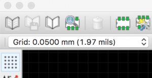
Dia 4.1: The grid size selector

In the upper left hand corner of the footprint editor, you will see a drop down menu that says something like “Grid: 0.0500mm (1.97mm)”. Click on it and a variety of sizes will appear for you to choose from. If the distance you need is not there; or if you want a grid of rectangles rather than squares, that’s not a problem! Simply choose “User Grid” from the drop down menu; then navigate to Dimensions (in the top toolbar) > User Grid Size. The Grid Properties window will pop up and you can set the dimensions to whatever you require.
Silkscreen Outline
So you have your pads in place, great! But your component isn’t just a few pads floating in midair; it has a body, and so your footprint should show that.
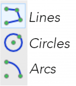
Dia 5.1: Silkscreen drawing tool icons

You’ll need this for PCB placement so you have an accurate visual representation of your component (you will be able to space your components nicely and they won’t overlap). We’ll draw the lines on the silkscreen layer.
There are 3 tools for drawing silkscreen lines (they are indicated by the icons with blue lines and green circles). We’ll focus on using the Add Graphic Line or Polygon tool (the one without curved blue lines in the icon). While the tool is active, your cursor will have a large white cross behind it. Now you’re ready to draw! Clicking once will start the line, clicking a second time will make an anchor point. ESC will cancel the current line segment. *Tip: Holding CMD while drawing will keep your lines straight and corners at 90° angles *Tip: With the tool drawing tool deselected, hitting E while hovering your cursor over a line segment will display line properties. Here you can change line thickness, and choose specific line start/end points. This is particularly useful if the datasheet needs specific sizes.
Saving and Exporting Your Footprint
You’re happy with your footprint? Great! Now you just need to save, export and you’re good to go.
Dia 6.1: The File drop down menu, providing options for saving your footprint

How you save your footprint depends on several factors; whether you already have a library to store your footprints in, and whether you have set this as the active library. We will assume you have not made a library yet in this case. Therefore, in the top toolbar, click File > Save Footprint in New Library (See Dia 6.1). You will greeted with a window which allows you to select the location for your new library (by default it will place it in your current project location). Whichever folder you choose to save in; the tool will create a folder with the same name with “.pretty” appended to the end.


